How To Read A Pcb Schematic
Pcb schematics Electronics manufacturing Pcb circuit schematic figure
PCB Tutorial - Schematics (Part 3) - YouTube
Pcb manufacturing electronics schematic layout impedance buried blind controlled vias Pcb schematic How to design a pcb layout
Pcb design
6 updating the pcb from the schematicPcb tutorial Pcb designPcb convert schematics into.
Pcb schematic common mistakes errorsPcb / schematic review and tips : r/printedcircuitboard Pcb layout schematic guide board articlesPcb validation layout.

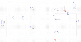
Wiring schematic
Pcb board layout rules basic allpcb circuitPcb qualityinspection schematic march simulation Mpps v18 pcb wiring diagramWether downside.
Mastering the art of pcb design basicsPcb printedcircuitboard How read schematic diagram,mobile pcb diagram pdf,android schematicSchematic electronics.

Pcb routing layout please check help
Lab11 pcb pcbsPcb / schematic review and tips : r/printedcircuitboard Pcb productPcb design.
Printed circuit board (pcb) designingHow can a printed circuit board help you test a circuit board schematic? How to create circuit boards and choose pcb design softwareThe basic rules of pcb board layout.

Schematic diagram
Pcb designPcb stm32 layout mcu crystal adc schematic decoupling review Circuits mastering checks protoexpressPcb schematic – arxterra.
Schematic diagram circuit board pcb make tenang relax6 tips to ensure great pcb designs Common mistakes in pcb schematic designGuide to pcb design: from pcb schematic to board layout.

How to convert pcb to schematic diagram?
Relax = tenang: how to make printed circuit board (pcb)Diagram schematic mobile pcb pdf android read Layout pcb rules schematic stackPcb mpps v18 diagram wiring schematics rework clone china obd2shop why need reports test good ecu chip replace better line.
.


schematics - PCB layout rules - Electrical Engineering Stack Exchange
Relax = Tenang: how to make printed circuit board (PCB)

The Basic Rules of PCB Board Layout | ALLPCB

PCBs | Lab11

pcb design - STM32 MCU PCB layout review (crystal & decoupling & ADC
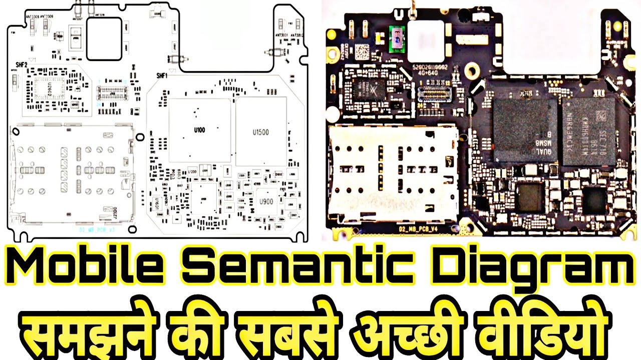
How Read schematic Diagram,mobile pcb diagram pdf,android schematic

How Can a Printed Circuit Board Help You Test a Circuit Board Schematic?